Scanning Electron Microscopy (SEM)
SEM Image Optimisation
At a neutral point of charge
Each of these currents is a function of the accelerating voltage, as shown schematically below. There exist two equilibrium (one stable and one unstable) points of nul charging:
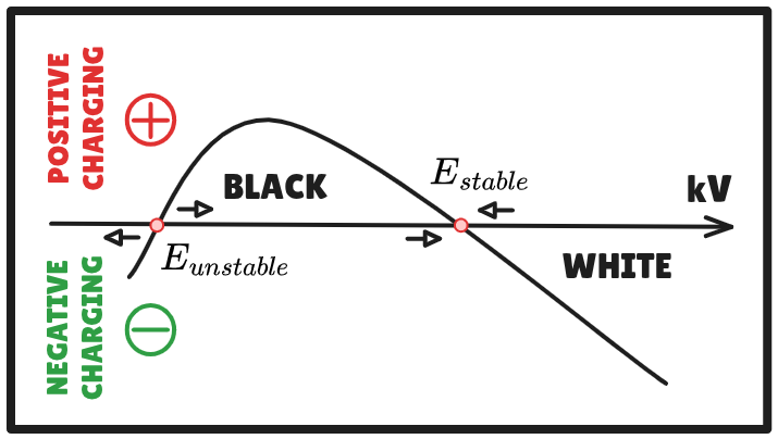
The sign of the surface charge influences electron deviation, but also the amount of scattered electrons reaching the detector. Thus, the following protocol is has been proposed by Dr. Ron Rasch:
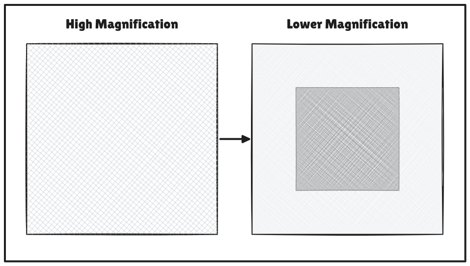
- Zoom to high magnification into a small rectangular zone and wait for maximal charging (counting to 10 in ones head)
- Zoom out and check the colour of the previously zoomed area
- If it is darker, increase kV, and if it is lighter decrease it.
For polymer species, this
SEM protocol for pristine and PEG-coated Daramic membranes
Sample preparation
Surface samples
- Cut approximately 5 × 5 mm pieces
- Dry the pristine and coated membranes fully at 70°C under vacuum
- Mount flat on aluminium SEM stubs with conductive carbon tape
Cross-sections
- Immerse membrane strips in liquid nitrogen
- Fracture them while cold
- Mount the fractured edge facing the beam
Conductive coating
Pt (for morphology imaging) thickness:
- Pt gives a fine-grained conductive coating and is suitable for high-resolution polymer imaging.
- Use carbon coating for EDS, (as Pt introduces strong Pt peaks)
JEOL JSM-IT810 parameters
| Parameter | Setting |
|---|---|
| Accelerating voltage | 1.9 kV (optimised kV-charging point) |
| Working distance | 7.8 mm |
| Detector | SE (scattered electrons) |
| Vacuum | 9.6x10⁻⁵ Pa |
| Probe current | 7 (on a scale from 1 to 14) |
| Scan | Use quick for focussing, stigmatisation and the wobbler at 7000x mag, the use fine. Adjust with averaging at a higher scan speed over 20 samples if surface charging is an issue. |
Surface orders of magnitude
- 200-500×: general morphology
- 2,000-5,000×: pore structure
- 10,000-30,000×: main comparison
- 50,000× or higher: fine pore/coating morphology
Compare density of surface layers between membranes.